
To someone who isn’t involved in power electronics design, it might seem unreal that the amount of power a component can handle depends more on how effectively waste heat can be removed from it than it does on the specific electrical ratings. Sure, the voltage and current ratings are important (especially the voltage rating), but the most important specs concern the thermal performance and limits. More specifically, it is the maximum allowed junction temperature and the thermal resistances that really dictate power rating.
For example, a few key specs from the datasheet for a modern Silicon Carbide (SiC) MOSFET in a standard TO-247 package will illustrate the point:
Maximum junction temperature: TJ[max] – 175° C
Maximum continuous drain current (with case @ 25° C): Id – 115 A
Drain-source on-resistance: RDS[on] – 16 mΩ typical; 28.8 mΩ max
Thermal resistance, junction to case: Rth[j-c] – 0.27° C / W
From this we can infer that the maximum allowed power dissipation with the case at 25° C is 555.5 W (from a 150° C rise in junction temp divided by the junction-to-case thermal resistance of 0.27° C / W). The power dissipated at 115 A can be found from Ohm’s law (W = I2 * R), which comes out to a range of 211.6 W at 16 mΩ to 380.8 W at 28.8 mΩ, for the typical and maximum values of drain-source on-resistance, respectively. So far, so good, as the junction temperature should only rise by 57.1 to 102.8° C over ambient, and we have 150° C of rise available. This is forgetting one very crucial detail, however: that thermal resistance spec assumes that the proverbial “infinite heatsink” is being used to keep the case at 25° C. In the real world, the thermal resistances of case to heatsink, and heatsink to ambient, can’t be ignored. Granted, these latter thermal resistances are totally outside the control of the component manufacturer, but when working backwards from the known parameters, it will be seen that the maximum allowed thermal resistance for the entire journey from junction to ambient is 0.394° C / W to maintain a 150° C rise in junction temperature at a possible 380.8 W of dissipation, and with 0.27° C / W of that already consumed by the junction-to-case thermal resistance, that leaves a paltry 0.124° C / W for both the thermal interface to the heatsink and the heatsink itself.
It is the maximum allowed junction temperature and the thermal resistances that really dictate power rating.
Parts in the TO-247 package often need an electrical insulator between their case and heatsink, and, unfortunately, good electrical insulators are often good thermal insulators. (To be fair, there are plenty of exceptions…like diamond, for example…what, that’s not practical?) One example of a high-performance electrically-insulating thermal interface pad material for this TO-247 package will add about 0.043° C / W of thermal resistance (given a pad thickness of 0.051 mm, a contact area of 2.1 cm2 and a material thermal resistance of 0.90° C – cm2 / W). This now leaves us with a mere 0.081° C / W of thermal resistance budget left over for the heatsink itself, and a quick perusal of the typical finned aluminum jobs available off the shelf—even when cooled by a gale-force wind—aren’t going to come within an order of magnitude of achieving that thermal resistance rating! There are some alternatives to the traditional finned heatsink that can achieve such a low thermal resistance from case to ambient, however, and we’ll discuss them following a quick detour to cover the ways in which heat causes failure (either eventually or suddenly).
Most electronics engineers are familiar with the rule of thumb that the lifespan of an electronic component is halved for every 10° C increase in its temperature. It is perhaps less well-known that this rule—which comes from the Arrhenius equation, named after the Swedish physicist/chemist and Nobel laureate—is the same one that describes how the rate of a chemical reaction changes with temperature. Of course, the Arrhenius equation only tells part of the story here: above a certain temperature, things will fail immediately, rather than just at a faster pace. For example, once the plastic dielectric in a film capacitor gets hot enough to melt, it’s game over (and spectacularly so). Similarly, semiconductors will fail to turn off (or remain off) above a certain temperature due to charge carriers (electrons and holes) acquiring enough energy to jump atomic valence bands, which then dislodges more carriers from other atoms until “avalanche conduction” occurs. Since the semiconductor device is supposed to be off, failure invariably occurs within a few nanoseconds from uncontrolled current flow. This is the same failure mechanism as when an excessive reverse voltage is applied to a semiconductor device, except in that case it is the electric field across the depletion region in the semiconductor junction that accelerates the charge carriers, rather than thermal energy. So: different proximate cause; same ultimate result.
Semiconductors will fail to turn off above a certain temperature due to charge carriers (electrons and holes) acquiring enough energy to jump atomic valence bands, which then dislodges more carriers from other atoms until “avalanche conduction” occurs.
Excessive temperature is an unsurprising cause of device failure, but perhaps less appreciated is the fact that cycling the temperature back and forth between, say, 30° C and 90° C, can cause device failure even more quickly than simply leaving it at 90° C continuously, due to thermal fatigue. In this failure mode, it is the difference in the coefficients of thermal expansion between each material in a device—such as between the silicon die and the die attach solder, or between the metallization on a film capacitor and the dielectric film itself—that sets up stresses at each interface that can cause tiny cracks to form. Typically these cracks afflict the least-compliant material first (e.g. the silicon die in a semiconductor device or the metallization in a film capacitor), but even more compliant materials like the die-attach solder are not immune to this failure mechanism. In the latter case, thermal cycling can open up any existing voids in the solder from imperfect application or wetting during the manufacturing process, which then leads to hot spots in the semiconductor. Hot spots are especially a problem for bipolar devices like IGBTs and pn-junction (or conventional) rectifiers, because in them the voltage drop across the junction declines with temperature. If a hot spot develops, then more current will get steered towards it, heating that spot up even more, and so on, until device destruction occurs. Unipolar devices like MOSFETs and Schottky rectifiers are largely immune to this failure mode because their on-resistance increases with temperature, so current is steered away from any hot spots that might develop.
Less appreciated is the fact that cycling the temperature back and forth between, say, 30° C and 90° C, can cause device failure even more quickly than simply leaving it at 90° C continuously, due to thermal fatigue-—caused by the difference in the coefficients of thermal expansion between each material in a device.
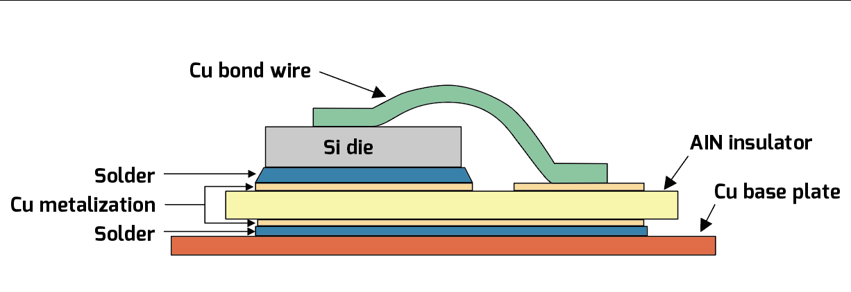
IGBT cutaway illustrating the multilayer construction of materials with different coefficients of thermal expansion
Minimizing the temperature swings in the key power-handling devices is a noble objective, but it’s not something that’s entirely under the control of the engineering design team. For example, the designers can’t control how much power will be demanded from the traction inverter at any given moment—they can only restrict the available power if the temperature climbs too high. Consequently, the most practical objective is simply to try to move the heat from the components generating it to the ambient as efficiently as possible, and as might be expected, the ways of doing this range from the mundane—like the natural convection heatsink—to the exotic—like immersion in a refrigerant. And as also might be expected, the complexity and/or cost of the more exotic schemes will often exceed the cost of simply adding more components in parallel (to both increase the raw power handling capability and spread the heat out over more area). It also bears mentioning that both the risk of failure, and the consequences thereof, go up with increasing complexity.
The natural convection heatsink is usually a plate of material with high thermal conductivity (e.g. copper, aluminum, aluminum nitride, etc) with many fins, pins, etc protruding from it to give it a high surface-area-to-volume ratio. The higher the thermal conductivity of the heatsink material, the farther heat will travel along it for a given temperature difference (i.e. between case and ambient). Since pure copper has a thermal conductivity of around twice1 that of the aluminum alloy most commonly used for heatsinks (6061-T6), it would seem to be the superior choice overall in this application, but copper is much more dense than it is thermally conductive, so the heatsink ends up being a lot heavier anyway, and furthermore, using copper is much more costly per unit weight than, say, simply adding a fan to a cheaper and lighter aluminum heatsink of the same size.
This segues nicely into the next step up in effectiveness, which is to blow air across the fins with a fan—aka forced convection—as even a little bit of airflow2 will dramatically reduce the thermal resistance (i.e. the reciprocal of thermal conductivity) of a given heatsink design (10x or better is easily achieved). As might be expected, the reliability is greatly reduced, both because a fan will fail much sooner than the chunk of aluminum it’s cooling, and because dust will accumulate on the heatsink fins/pins much more rapidly, leading to a progressive increase in thermal resistance unless regularly cleaned.
CPU cooler heat pipe application
The heat-removal method most likely to be employed when a lot of heat is produced in a small volume (such as the traction inverter) is the “cold plate.” This is simply a block of aluminum, copper or other thermally-conductive material through which a liquid coolant is circulated (usually along a serpentine or multiply-parallel path) which conveys heat to a fan-cooled radiator located some distance away. This scheme combines forced conduction (via the pumped coolant) and forced convection (via the fan on the radiator) so it is far more expensive and a lot more prone to failure than the fan-cooled heatsink solution, but it can reduce thermal resistance by about another 10x, which is necessary if trying to remove more than about 50-75 W of heat per TO-247 size package (i.e. – approximately 200 mm2 of contact area), and there are a whole bunch of them to cool, for example.
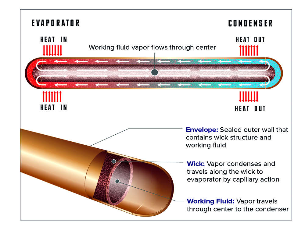
Finally, there is the most exotic scheme—though not necessarily the most complex, as we’ll soon see—which is to use a coolant (or refrigerant, to be more precise) with a boiling point that is above the highest expected ambient temperature, but sufficiently below the maximum junction temperature to account for the thermal resistance from junction to case. This is called phase-change or vapor-state cooling, and it relies on the principle that most liquids require considerably more heat energy to change from a liquid to a gas at their boiling point (aka their latent heat of vaporization) than it takes to raise the temperature of the liquid by one degree (aka their specific heat). For example, water requires about 500x more energy to vaporize at 100° C than it does to go from, say, 99° C to 100° C! While a full-blown mechanical refrigeration system (e.g. using a compressor, etc) would be a very complicated way of implementing phase-change cooling, you can get all of the benefits without the hit to reliability by using heat pipes, which are sealed copper tubes with a roughened interior surface, and which most commonly contain a small amount of water under a partial vacuum so it will boil at less than 100° C.
How a heat pipe works.
Image courtesy of Advanced Cooling Technologies, Inc.
When heat is applied to one end of a heat pipe, the water inside boils, and this vapor travels to the other end of the tube, to which is attached a natural- or forced-convection heatsink, where it condenses.
When heat is applied to one end of a heat pipe, the water inside boils, and this vapor travels to the other end of the tube to which is attached a natural- or forced-convection heatsink, where it condenses. The roughened interior surface then conveys the liquid back to the hot end via capillary action (and gravity, if oriented properly) where the cycle repeats. This is so effective at moving heat that if you hold a 6-8 mm diameter x 150-200 mm long heat pipe in your hand, you can use it slice through an ice cube in record time (or for as long as your hand can withstand the freezing cold conducted to it, anyway). Consequently, a heat pipe can allow the use of a natural- or forced-convection heatsink to cool devices running at such a high heat flux (or amount of heat per unit area) that a cold plate would otherwise be required, but without the pump, coolant reservoir, etc, hence this massive increase in effectiveness is also more reliable, overall. Heat pipes are a rare case of a win-win situation in engineering, and highly recommended for dealing with the most vexing heat-removal problems.
This article appeared in Issue 61: Jul-Sept 2022 – Subscribe now.
Source: Charged EVs